About Us
HomeAbout Us

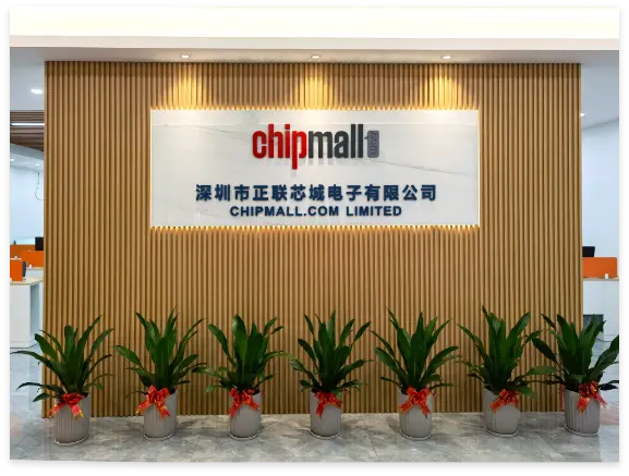
Company
Profile
Founded in 2006 and located in Shenzhen, China Chipmall.com is a world-renowned electronic component distribution platform, distributing electronic products from more than 500 branded manufacturers with a variety of semiconductor products, passive devices,interconnected devices and electromechanical components.
Chipmall.com always adheres to the principle of "Quality first, customer first" and has been recognized by many customers.
In the future, we will continue to improve the company's processes and services, committed to meet the continuous growth of customer needs, to become your most trusted partner.
OUR SERVICE

DISTRIBUTION

PRODUCT
PROMOTION

INVENTORY
MANAGEMENT


LET'S US LEARN ABOUT
THE CORPORATE CULTURE
Create value with service, establish authority with professionalism and win the future with integrity.
 Our Vission
 Our Mission
 Core Values
QUALITY
ASSURANCE
Chipmall realized there are many fake parts in the global electronics supply chain.which would have caused serious issues and bad consequences for customers.Therefore, we firmly believe that only by obtaining sources from authorized suppliers with enhanced quality test could it be safe and reliable.
Read More
Milestone

OUR TEARMS